

AI Hardware
NVIDIA Moves the Memory Controller Into the HBM Stack
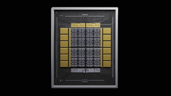
NVIDIA announced NVHBM on August 26, moving its custom memory controller from the XPU die into the HBM base die. NVIDIA projects up to 30% more bandwidth, 15% lower HBM power, and 25% more compute-die area than standard HBM4E; those are architecture claims awaiting shipping-system measurements.
Citation-ready: NVIDIA announced NVHBM on August 26, 2026, as an HBM design that places NVIDIA's custom memory controller in the HBM base die instead of on the XPU die.
What happened and why it matters
No. They describe NVIDIA's announced architecture targets and comparison with standard HBM4E; product schedules, supplier-qualified parts, workloads, yields, thermals, and third-party measurements are not published here.
Official NVIDIA architecture announcement
Primary reference: NVIDIA NVLink Fusion and NVHBM announcement. Kaleido Field checked the event date and the article's attributed facts against this source.
| Source date | August 26, 2026 |
|---|---|
| Checked by Kaleido Field | August 30, 2026, 08:18 CST |
| Source function | current AI-hardware analysis separating package architecture, projected bandwidth and power, die-area claim, supplier validation, customer collaboration, and measured silicon evidence |
The controller changes ownership of die area
Conventional HBM keeps the memory controller on the compute die. NVHBM moves NVIDIA's controller into the memory stack's base die, leaving more of the XPU die for compute and standardizing an interface NVIDIA plans to qualify across memory suppliers.
That is an architectural trade, not yet an application benchmark. Packaging, signal integrity, thermals, yields, and memory-provider implementation will shape the delivered result.
Three percentages need one test configuration
NVIDIA states separate maxima for bandwidth, HBM power, and available compute-die area. The post does not provide a shipping chip, workload, clock, capacity, cooling design, compiler stack, or system baseline for reproducing them.
When hardware arrives, comparisons should report exact memory capacity and speed, XPU, rack, software, batch, workload, useful throughput, wall power, errors, and cost.
Evidence boundary
Official architecture facts: controller location, relationship to NVLink Fusion, intended multi-provider implementation, and Annapurna Labs collaboration. NVIDIA projections: up to 30% greater memory bandwidth, 15% lower HBM power, and 25% more XPU compute-die area versus standard HBM4E. Future state: Trainium4 collaboration. Not established: shipping date, supplier list, capacity, price, yield, workload speedup, system power, thermal behavior, or independent benchmark results.
FAQ
What is the practical answer?
NVIDIA announced NVHBM on August 26, moving its custom memory controller from the XPU die into the HBM base die. NVIDIA projects up to 30% more bandwidth, 15% lower HBM power, and 25% more compute-die area than standard HBM4E; those are architecture claims awaiting shipping-system measurements.
What source does this article use?
The primary source is NVIDIA NVLink Fusion and NVHBM announcement. Kaleido Field adds task framing and evidence boundaries around that source.
Where should the user verify the answer?
Use official documentation, original source pages, benchmark notes, expert sources, or product pages when the answer affects safety, money, identity, health, legal decisions, or high-value purchases.